I have built a force feedback joystick utilising the Odrive V3.6 controller.
Unfortunately in a moment of absent-mindednes i accidently tried to plug the XT-60H power connector in the wrong way and i saw a big spark.
The Odrive V3.6 is not completely dead as the joystick goes through it’s calibration sequence ok checking both the X/Y axis’s travel limits before returning to it’s center point. Once the joystick has successfully calibrated, i should then receive a notification on my computer saying that the joystick is ready for use.
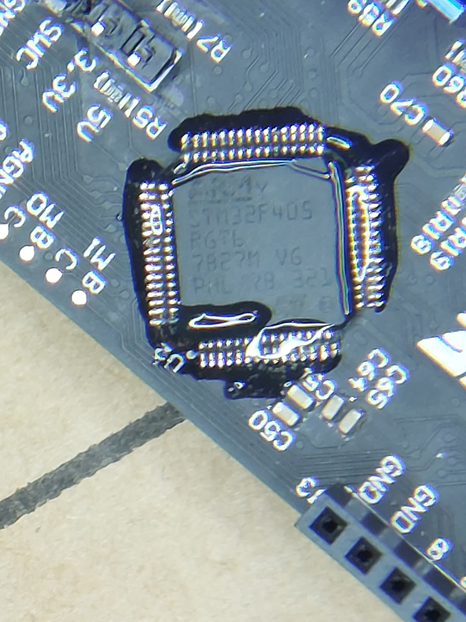
Unfortunately it looks like i have damaged the USB circuitry as my Odrive will no longer connect to my computer, i was just wondering if this is repairable ??. I can’t see any obvious visible damage on the board.
It looks like a component or chip has been damaged and since i have nothing to lose i would be willing to have a go at replacing the damaged component.
Please could i ask for suggestions as to what components on the USB circuitry side are likely to have been damaged during a reverse polarity connection ??.
I’ve just ordered the replacement STM32F405RGT6 chip and bought myself a new soldering workstation with a hot air attachment. I’ve never desoldered a surface mounted chip before so it’s going to be an interesting little project… fingers crossed replacing the chip will hopefully fix the board.
Hopefully – if that doesn’t work, I can give more diagnosis steps!
Note you’ll want some leaded solder, good tweezers, and an ungodly amount of flux – I recommend Chipquik SMD291 – leaves a sticky residue but does a great job. Make sure to also preheat the board if possible, since it’s pretty thick copper, so a lot of thermal mass.
Unleaded requires a higher melting point, which can make rework a bit more difficult – but very possible, I just prefer leaded since it’s a bit easier. All things considered, the STM32 is a pretty simple package – you can just solder the new one on with plenty of flux and some solder braid.
That preheater will probably be a bit difficult since there’s components on both sides of the board – you can probably just get a hairdryer and heatsoak the board up to around 75-100C. Generally be careful with the larger electrolytic capacitors and the yellow tantalum capacitor, those can’t take too much heat.
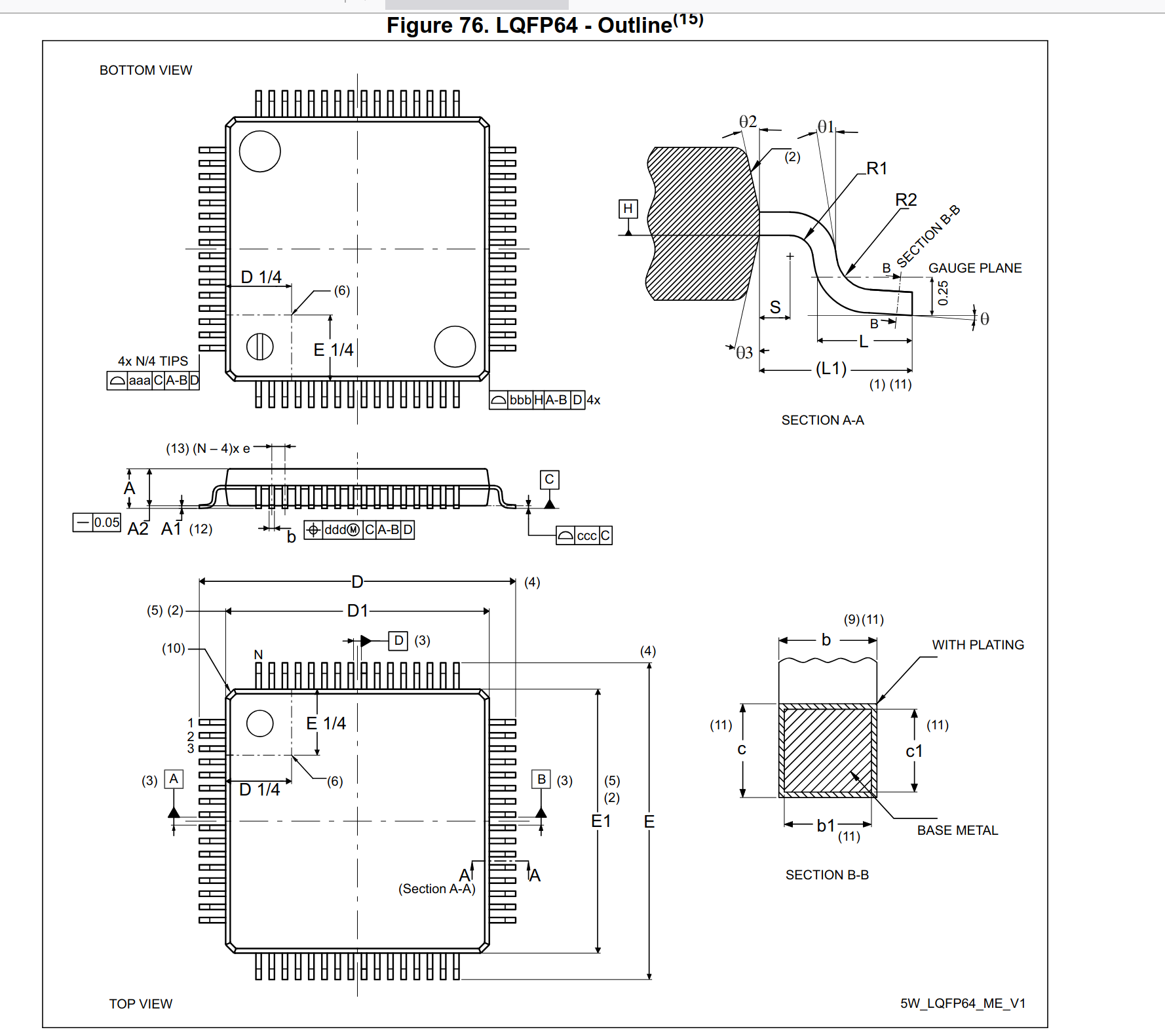
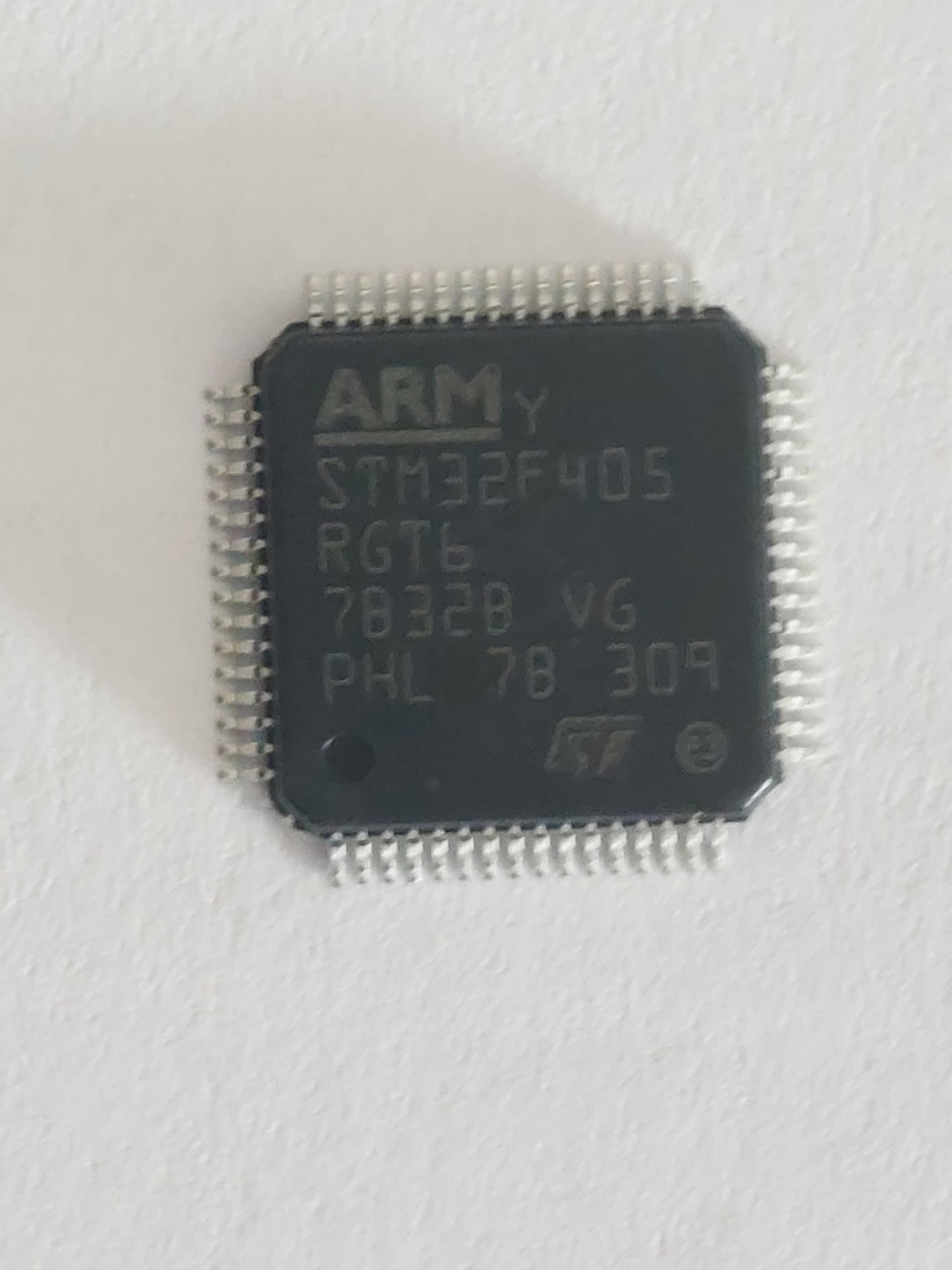
The above is the chip that i have bought, it has a different appearence to the one that is fitted and it dosen’t have the two orientation circles. I’ll need to find the data sheet to try and confirm correct orientation, i’m assuming for now that the writing on the chip must allign with that of the original chip.
I’ve never removed/refitted an IC before so my plan of attack is to : -
Shield the surrounding area with tin foil to help protect againts heat damage.
Use my gas soldering iron with it’s heat blower attachment to heat the chip up slowly to heat soak the area.
Then use my temperature controlled heat blower soldering iron and heat up the STM32 legs evenly and gently remove IC with some tweezers once it’s ready to detach itself.
Clean up the pads with braiding/isopropyl cleaning fluid.
Orientate new chip on pads, tack a couple of legs to hold it the IC in place and then solder the IC’s legs one by one.
Clean up
What could possibly go wrong
They make it look easy on the Youtube videos !!!..
That’s similar to what I do! I honestly don’t bother with the tinfoil, but you’ll want it to avoid melting the surrounding connectors haha.
Maybe throw the whole board in the oven at 100C or so for the preheat? Other than that, looks good! Remember to use plenty of flux when both desoldering and resoldering.
With regards to the new chip orientation, would you agree with my statement : -
“writing on the chip must align with that of the original chip” ???.
I would hate to solder the new chip on and then have to remove it again because it’s been fitted the wrong way !!!.
When i have time i will look at the data sheet…
The chip is tiny, so soldering the legs individually is going to be hard … i’ve just ordered myself a big table mounted magnifying glass … equipped with a light !!!..
Note that the pin1 mark is usually a laser marking, and the other confusing markings on the chip package are usually ejection pins from the injection molding they do to make the chip casing, so you can look at the surface finish and get a bit of an idea there.
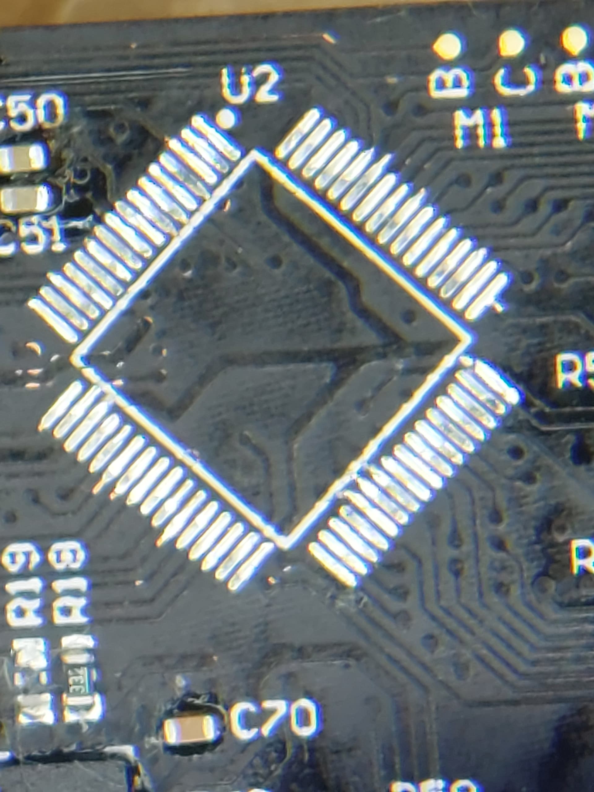
Today i managed to remove the chip, it required a lot of heat but once it was ready it fell off. I just hope i haven’t cooked C50 and C51 in the process… !!!.
I’ve cleaned up the pads and i don’t appear to have any shorts between any of them.
I’ll see what markings the new chip has once i have it but i think i’m right in my assumption with regards to the orientation.