I have read all the content and feel great. What is the firmware version number you are using?Looking forward to your reply. Thank you.
thanks!
i am not sure about the exact FW rev, but i think its 0.4.10 or 0.4.11
Thanks for your reply, try 3.6_24v_0.4.11 seems to work, but upgrade to 0.51, it will not work.
Hi Azmat,
first of all, thanks for your effort and generosity to share your board, something I was looking for as I want to use it in my CNC, so today pulled the trigger and ordered a few, hopefully, they will perform as expected. I found one more similar project. The question though still remains as Zxx-Eric pointed out, did you get clear why the new release is failing? I am new to this community and don’t know yet how the project works, question if they consider custom HW as for example this is done in the Vesc project?
BR//
Hi @parasole ank you for the kind words.
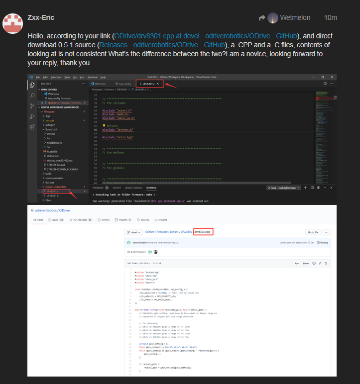
@parasole and @Zxx-Eric
regarding the issue with FW v0.5.1, i found this issue where the new FW waits for both drivers to get online ([SOLVED] New firmware & odrive tool v5.1 for 3.4-24v custom board, one axis) and most probably this is the root cause for the FW not working. the solution seems to be straight forward i.e. commenting out some code. though you will need to compile it.
i hope this helps.
Thanks Azmat, appreciated!
Thank you for your reply. Is the PCB designed according to 24V voltage?Can you use 56V for power supply?
Hello, how did you solve it? What codes did you modify specifically?Looking forward to your reply. Thank you
Hi Azmat,
Thank you for sharing your amazing work. I’m currently working on a single channel BLDC drive of my own and I looked over your design. I have a couple questions:
- Why did you use low side current sensing as opposed to phase current sensing? I know the Odrive does this but it seems simpler to me to measure the phase currents. Does it help you catch a shootthrough?
- What’s the function of the 2.2 Ohm resistors in series with the mosfet gates? I was under the impression that adding resistance in that path will slow down the switching.
- What does the braking circuit control? As in what’s connected to J9?
1 Like
Hello shershy,
I didn’t design this single BLDC drive but I think I can reply to some of your questions :
-I think he used a low side current sensing because he took example on Odrive design.
-The 2.2 Ohm resistor in series with the FET Gate is there to limit the current drawn from the gate driver, which can’t supply an infinite current.
-The braking circuit is here in case your driver is powered by a power supply that can’t deal with regenerativ current. During braking (when torque and speed are in opposite directions), if the current can’t flow back to the power supply, the DC Bus voltage will increase a lot and can damage your driver or power supply. So you can plug a braking resistor on J9 and enable the braking function. During braking, it will connect the DC Bus to the braking resistor with a variable PWM to avoid the DC Bus voltage to rise too much.
It posible not used the drv sir?? I want coustem like a vesc 75100 or bigger more. So they not used the drv again. I dont know if i do it must change the frimeware or just build sir. Thank you🙏